
Security in I/O
Overview
I/O interfaces form the physical boundary of the system and are therefore one of the most exposed and vulnerable attack surfaces. Attackers can manipulate signals, inject faults, spoof sensors, probe pins, or exploit electrical weaknesses to gain access or alter system behavior. Security analysis focuses on:
- protecting I/O paths from tampering
- ensuring authenticity and plausibility of external data
- detecting abnormal electrical or logical patterns
- preventing fault‑injection‑based bypasses
- isolating compromised external devices
I/O security is the first line of defense against physical and semi‑physical attacks.
I/O Threat Surface
The I/O subsystem exposes multiple attack vectors:
- GPIO: spoofing, probing, forced transitions
- UART/SPI/I²C: replay, injection, bus takeover
- LVDS/SerDes: glitching, timing manipulation
- Reset/config pins: forced resets, mode switching
- Analog inputs: sensor spoofing, bias injection
- High‑impedance states: signal injection, bus hijacking
Figure 1 — I/O Threat Surface Map

Conceptual map showing the attack surface across GPIO, serial buses, analog inputs, reset/config pins, and high‑impedance states.
Main Security Threats
1. Signal Spoofing
Injecting forged sensor values or control signals to manipulate system behavior.
2. Tampering on External Lines
Pulling lines high/low, forcing transitions, or altering voltage levels.
3. Probing and Eavesdropping
Physically accessing pins to read or manipulate data.
4. Fault Injection Attacks
Glitches, voltage dips, timing faults, EM pulses, or laser‑induced faults.
5. Replay Attacks
Reusing previously valid sensor data or control frames.
6. Short‑to‑Battery/Ground as Attack Vector
Forcing electrical faults to trigger unsafe or unexpected states.
7. Side‑Channel Leakage
Extracting information from timing, power, or EM emissions.
8. Configuration Register Manipulation
Changing I/O modes, thresholds, pull‑ups, or drive strength.
9. I/O Buffer Abuse
Exploiting weak drive strength or high‑Z states to inject signals.
Figure 2 — Fault Injection on I/O Lines
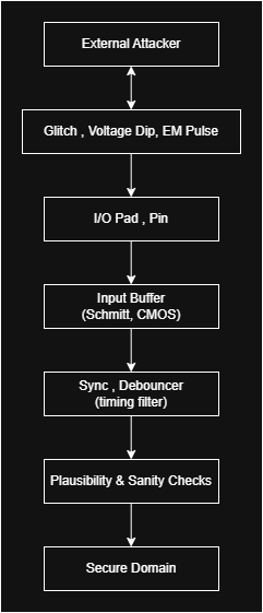
Example of glitch, voltage dip, and timing‑fault injection paths targeting I/O buffers and input synchronizers.
Mitigation Techniques
1. Input Authentication
Ensuring that external data originates from trusted devices.
2. Signal Plausibility Checks
Verifying that sensor values follow expected physical behavior.
3. Electrical Anomaly Detection
Monitoring current, voltage, impedance, and edge rates.
4. Glitch and Fault‑Injection Protection
Filtering, debouncing, metastability hardening, and timing supervision.
5. Secure Configuration Registers
Locking I/O modes, thresholds, and pull‑ups after initialization.
6. Redundant Sensing
Comparing multiple sensors or acquisition paths to detect spoofing.
7. Shielding and Routing Protection
Reducing exposure to probing and electromagnetic attacks.
8. End‑to‑End Integrity Checks
CRC, MAC, or digital signatures on data entering through I/O.
9. Isolation and Sandboxing
Limiting the impact of compromised external devices.
10. Built‑In Self‑Test
Validating I/O logic, thresholds, and buffer integrity.
Figure 3 — I/O Sanitization Pipeline
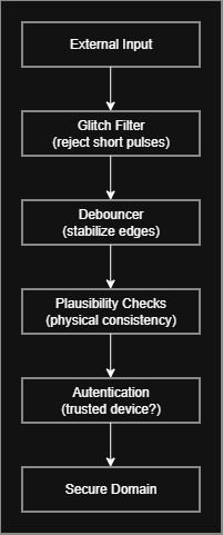
Pipeline showing raw external input → glitch filter → debouncer → plausibility checks → authentication → secure domain.
I/O Monitoring and Diagnostics
Security monitoring for I/O includes:
- Edge‑rate monitors Detect abnormal rise/fall times indicative of probing or injection.
- Glitch detectors Identify pulses too short to be legitimate.
- Illegal‑transition detectors Catch transitions outside expected timing windows.
- Timeout monitors Detect stuck‑high/low or missing activity.
- Protocol‑level sanity checks Validate framing, CRC, sequence numbers, and timing.
Figure 4 — I/O Tamper Detection Architecture

Architecture combining electrical monitors, timing supervision, and protocol‑level checks to detect tampering attempts.
Secure Reset and Configuration Paths
Reset and configuration pins are high‑value targets:
- forced resets
- mode switching
- bypassing secure boot
- disabling protections
Mitigations:
- secure reset filters
- authenticated configuration
- one‑time lock registers
- tamper‑resistant routing
Figure 5 — Secure Reset Path
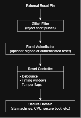
Secure reset architecture with glitch filtering, authentication logic, and tamper‑resistant routing.
I/O Isolation and Containment
When an external device is compromised, the system must:
- isolate the affected I/O
- prevent propagation into the secure domain
- log and classify the event
- trigger safe fallback modes
Figure 6 — I/O Isolation and Containment Flow
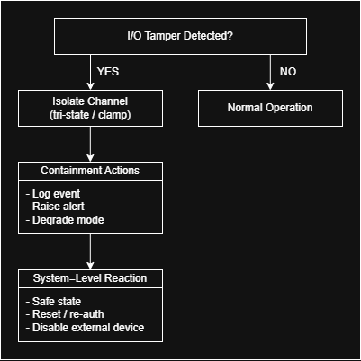
Flow showing detection → isolation → containment → system‑level reaction.
