
⭐ Safety in Digital I/O
Safety in Digital I/O
Introduction
Digital I/O pins form the electrical boundary between the chip and the external world. Because they directly interact with actuators, sensors, and communication lines, they represent a critical point of failure in safety‑related systems.
This page describes the failure modes, diagnostic mechanisms, and architectural strategies used to ensure safe operation of digital I/O.
Failure Modes in Digital I/O
Digital pins can experience several classes of hardware faults. These faults may originate at the pad, inside the I/O cell, or in the internal routing (I/O MUX).
Pad‑Level Faults
- Stuck‑high — output permanently at logic ‘1’
- Stuck‑low — output permanently at logic ‘0’
- Open circuit — pin disconnected or floating
- Short‑to‑ground — forced low regardless of logic
- Short‑to‑battery — forced high regardless of logic
- Short‑to‑adjacent pin — bridging faults
- ESD‑induced degradation — partial or intermittent failure
I/O MUX Faults
- Incorrect MUX selection — pin routed to the wrong peripheral
- Stuck MUX — impossible to change the pin function
- Glitch during MUX switching — transient routing to unintended logic
- Internal cross‑connection — two peripherals internally connected to the same pad
- Configuration corruption — SEU, brown‑out, or ESD altering MUX registers
Pad Configuration Faults (Voltage / Current / Drive)
Modern pads are highly configurable. Faults in these settings can create unsafe behavior:
- Wrong voltage domain — pad configured at 1.8 V but connected to a 5 V bus
- Incorrect drive strength — too weak (signal integrity issues) or too strong (overstress)
- Incorrect slew rate — excessive EMI or timing violations
- Pull‑up / pull‑down misconfiguration — floating inputs, unintended logic levels
- Input buffer disabled — pin appears stuck or open
- Output buffer enabled unexpectedly — bus contention, short‑circuit risk
Figure 1: Digital I/O Failure Modes Overview

Overview of pad‑level, MUX‑level, and pad‑configuration failure modes affecting digital I/O safety.
Why MUX faults matter
The I/O MUX determines which internal peripheral is electrically connected to the pad. Because it sits between the pad and the internal logic, a MUX fault can silently redirect signals, bypass diagnostics, or disable safety‑critical paths.
MUX faults matter because they can:
- Bypass safety mechanisms A pin intended for GPIO safety monitoring may be accidentally routed to a peripheral output.
- Disable sensing paths If the input buffer is disconnected, plausibility checks and loopback diagnostics become ineffective.
- Create unintended actuation A peripheral output (PWM, SPI, UART TX) may be routed to a pad that drives an actuator.
- Break redundancy Two redundant sensors may be internally cross‑connected, invalidating diagnostic coverage.
- Escape boundary‑scan detection JTAG sees only the pad; internal routing faults are invisible externally.
- Be altered by SEU or brown‑out MUX configuration registers are vulnerable to corruption.
In short: MUX faults are dangerous because they are internal, silent, and often undetectable from the outside.
Figure 2: I/O MUX Faults and Signal Routing

Internal routing faults caused by incorrect MUX selection, stuck MUX, switching glitches, cross‑connections, or configuration corruption.
MUX‑in and MUX‑out Directions
The I/O MUX handles routing in two independent directions, each with its own failure modes and diagnostics.
MUX‑in direction (Pad → Internal Logic)
This path determines which internal block receives the signal from the pad.
Failure modes:
- wrong peripheral receives the input
- input buffer disabled
- pull‑ups/pull‑downs misconfigured
- internal cross‑connection
- SEU corrupting input routing
MUX‑out direction (Internal Logic → Pad)
This path determines which internal block drives the pad.
Failure modes:
- unintended peripheral drives the pin
- GPIO output disabled or overridden
- output buffer enabled unexpectedly
- wrong voltage/current configuration
- glitch during switching between functions
Figure 3: MUX‑in vs MUX‑out Signal Paths

Separation between input routing (pad → internal logic) and output routing (internal logic → pad), highlighting distinct failure modes and diagnostic needs.
Diagnostic Mechanisms
Safety‑critical systems use several techniques to detect digital I/O faults:
- Boundary Scan (JTAG) — detects open/short at board level
- Internal loopback paths — verify output → input consistency
- Read‑back of output drivers — confirm the driven value matches the intended one
- Current sensing — detect short‑to‑ground or short‑to‑battery
- Pull‑up/pull‑down monitoring — detect open circuits or floating states
- Pin plausibility checks — compare expected vs actual state
- Configuration read‑back — verify MUX and pad settings are correct
- SEU monitoring — detect corruption of I/O configuration registers
Figure 4: Digital I/O Diagnostic Architecture
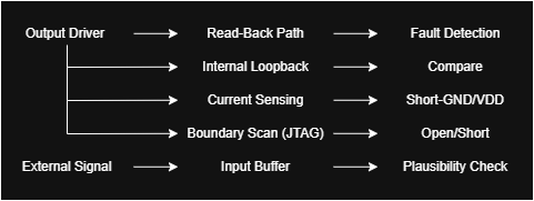
Internal and external diagnostic mechanisms used to detect digital I/O faults, including read‑back, loopback, current sensing, boundary scan, and plausibility checks.
Safety Architecture Considerations
Digital I/O safety interacts with several architectural elements:
- FCCU — reporting pin‑level faults
- Safe states — forcing outputs to a known safe configuration
- Watchdog — supervising I/O‑driven actuators
- Redundant sensing — cross‑checking external signals
- Protocol layers — validating I/O‑driven communication
- Pad configuration integrity — ensuring voltage/current settings remain valid
- I/O MUX integrity — ensuring routing cannot silently change
